This, so that we can properly compare the two consoles, is the naked motherboard of the Xbox 360 console (again from PC WATCH IMPRESS):

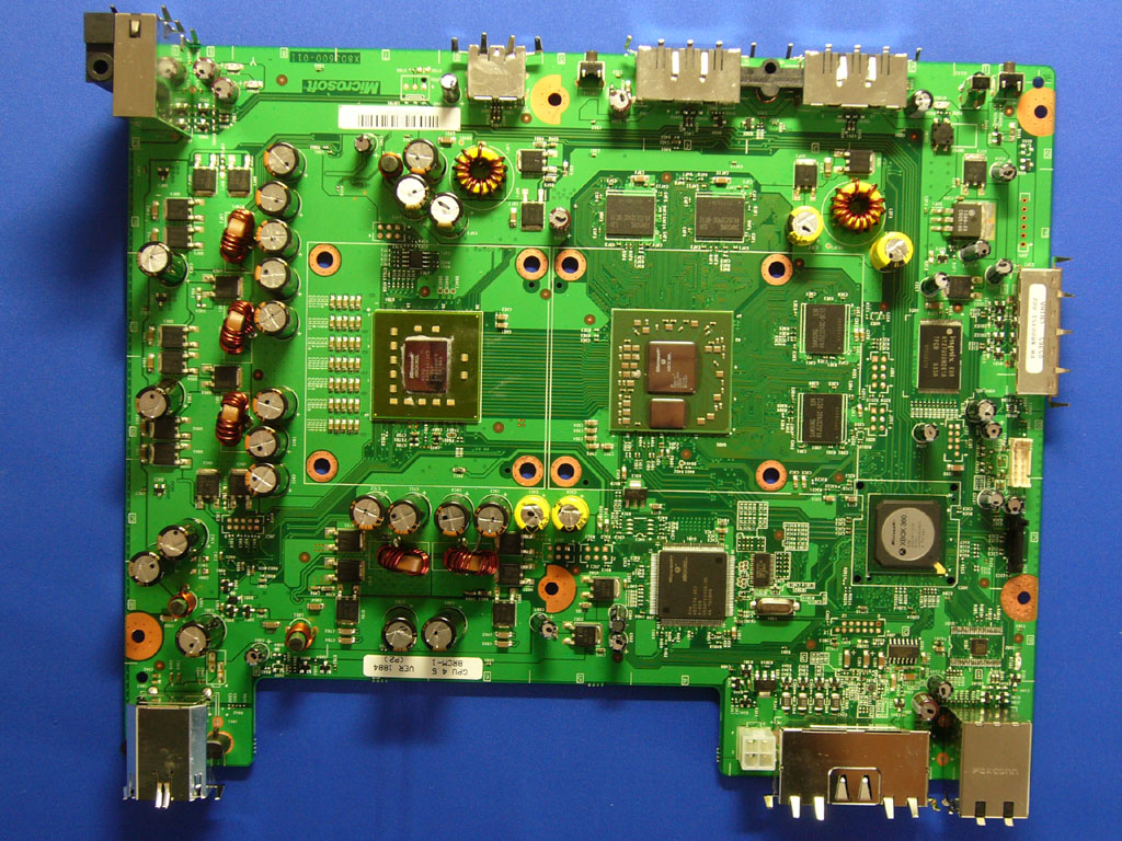
On the left you can see Xbox 360's CPU called Xenon (or Waternoose) and on its right you can see Xbox 360's GPU called Xenos (or C1) with its attached E-DRAM module (this daughter die is on the same package as Xenos, but on a different die).
Another thing we should notice is how the central piece of the equation in Xbox 360 is not the Xenon CPU, but Xenos. Xenos is both the GPU and the system's North-bridge, it is where the main memory controller is located and if you look around it you can see it being surrounded by the 4x1024 Mbits GDDR3 memory chips with a 128 bits bus clocked at 700 MHz delivering about 22.4 GB/s of transfer speed. The high speed link that connects CPU and GPU manages a peak of almost 22 GB/s and we ought to remember that Xenos can ask Xenon to lock a portion of its L2 cache to read/write from/to it. Looking more on the lower-right side of the motherboard we can see the Xbox 360's South-bridge, its I/O processor which was designed by VIA and you can spot it by that silver filled circle on its surface (trivia: the Video Scaler chip inside the Xbox 360 was designed internally at Microsoft by a group of talented engineers which, one upon a time, got its hands dirty with another famous project.... the M2).
Another thing we should notice is how the central piece of the equation in Xbox 360 is not the Xenon CPU, but Xenos. Xenos is both the GPU and the system's North-bridge, it is where the main memory controller is located and if you look around it you can see it being surrounded by the 4x1024 Mbits GDDR3 memory chips with a 128 bits bus clocked at 700 MHz delivering about 22.4 GB/s of transfer speed. The high speed link that connects CPU and GPU manages a peak of almost 22 GB/s and we ought to remember that Xenos can ask Xenon to lock a portion of its L2 cache to read/write from/to it. Looking more on the lower-right side of the motherboard we can see the Xbox 360's South-bridge, its I/O processor which was designed by VIA and you can spot it by that silver filled circle on its surface (trivia: the Video Scaler chip inside the Xbox 360 was designed internally at Microsoft by a group of talented engineers which, one upon a time, got its hands dirty with another famous project.... the M2).
No comments:
Post a Comment