I think that clean motherboard designs are something to be really appreciated given how much work goes into them and how easy it is to rush the design late in the manufacturing process to meet a deadline.
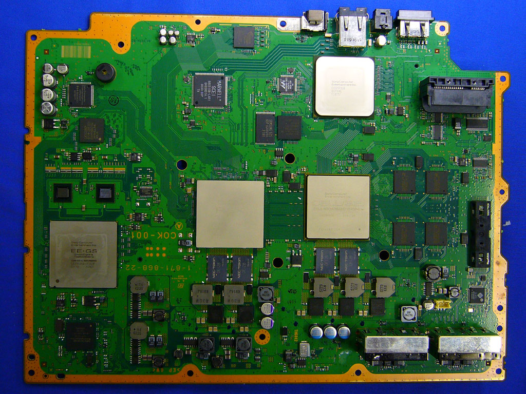
The main four chips you see on the first picture on the right (which is a shot of PLAYSTATION 3's mother-board taken by the chaps at PC WATCH) are from up-right to bottom-left:
1.) It is the I/O Bridge chip or I/O Processor: as you can see it has a quite fat connection with the CELL processor which sits right below. As this next diagram (taken from a Sony Computer Entertainment presentation) shows the I/O Bridge is in charge of the Ethernet link, of the USB 2.0 ports, of the Blu-Ray disc drive as well as the Memory Card slots, management of the Wireless LAN chip (provided by Marvell), HDD controller management, etc... it is basically PLAYSTATION 3's South-bridge chip. The chip's code is CXD2973GB.
2.) The second chip, in order, sitting below the I/O processor is the now very famous CELL Broadband Engine processor, the CPU, the heart of the console: to its right we can see the four 512 Mbits XDR memory modules delivering a
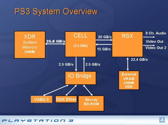 whopping 25.6 GB/s of bandwidth and to its left we can see the 35 GB/s connection (a 20 GB/s channel delivering data to RSX from CELL and a 15 GB/s channel delivering data from RSX to CELL) to the system Graphics Processor code-named RSX. You can see how Rambus's patented FlexPhase technology allows the data and multiplexed command+address traces to be laid out in a flexible and simple way (rest of PR speech is here ;)). The CPU code is CXD2964GB.
3.) To the left of the CELL processor we have the graphical powerhouse of PLAYSTATION 3, the nVIDIA co-developed Reality Synthesizer or RSX (an enhanced version of the nVIDIA GeForce 7 architecture shrunk using 90 nm technology and optimized for use with the CELL processor in PLAYSTATION 3). If you wonder "well, where has the Video RAM or VRAM run off to ?" do not worry as it is embedded in the same package as RSX's die as shown by further photos you can find here
4.) The last, but not least of the four major chips present in the PLAYSTATION 3's mother-board: it is the integrated EE+GS chip. This Integrated Circuit or IC combines in one single silicon surface (or die) the Emotion Engine (or EE, the CPU of PlayStation 2) and the Graphics Synthesizer (or GS, the GPU of PlayStation 2) using 90 nm technology: the chip has always been known as EE+GS@90 nm. From what I hear, this is not exactly the same EE+GS chips produced initially for the PSX device (only released in Japan) and used also in the slim-line PSTwo consoles, but a newer and modified incarnation. The code of this EE+GS chip is CXD2953AGB.
Not just the EE+GS chip made it in PLAYSTATION 3, look above it and compare those two very little chips with what you see in the following photo (again from PC WATCH IMPRESS, a slim-line PSTwo's motherboard photo):
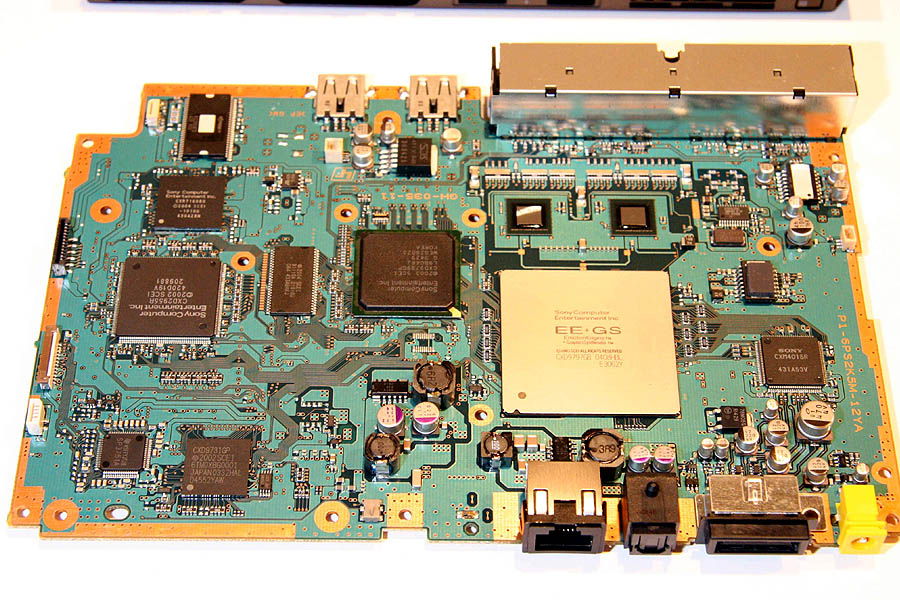
That's right folks, SCE included 32 MB of Direct Rambus DRAM along with the EE+GS combo chip thus bringing over also the system RAM used by PlayStation 2. PlayStation 2's memory layout was roughly: 32 MB of Direct Rambus DRAM (system RAM), 4 MB of embedded DRAM (VRAM), 2 MB of RAM for the SPU2 sound processor and 2 MB of RAM for the I/O CPU.
Sony Computer Entertainment (or SCE) was not able to complete a PlayStation 2 software emulator solution that satisfied their backward-compatibility needs as there are quite a few challenges emulating the characteristics of PlayStation 2's powerful Graphics processor (the GS). PlayStation/PSOne backward-compatibility quite likely is not the headache-inducing problem for SCE as PlayStation 2/PSTwo backward-compatibility is: in PlayStation 2 the original PlayStation 's GPU was already emulated through the GS (display lists were pre-processed by the EE before they were forwarded to the GS which included some hardware features to ease the emulation process).
It should be noticed that since PSTwo's latest revisions (series SCPH-7500x IIRC) the former PlayStation/PSOne CPU, which had been used as PlayStation 2's I/O processor (also known as IOP), was substituted by a newer (and PowerPC based according to an interview with an IBM executive a while ago) processor which took the duty of emulating the IOP and the PlayStation 2 Sound Processor (which is called SPU2).
I do not think that it would surprise many people to hear that the problems some PSOne and PSTwo games experience running on these latest model PSTwo's are I/O and Sound ones ;).
Sony has enough knowledge of every little detail concerning PSOne architecture and its quirks as well as all the processing power they need to efficiently emulate PSOne titles purely in software: it is not rocket science any longer even on PC's quite less powerful than PLAYSTATION 3.
No comments:
Post a Comment